- 您现在的位置:买卖IC网 > Sheet目录323 > DSP56311EVM (Freescale Semiconductor)KIT EVALUATION FOR DSP56311
�� �
�
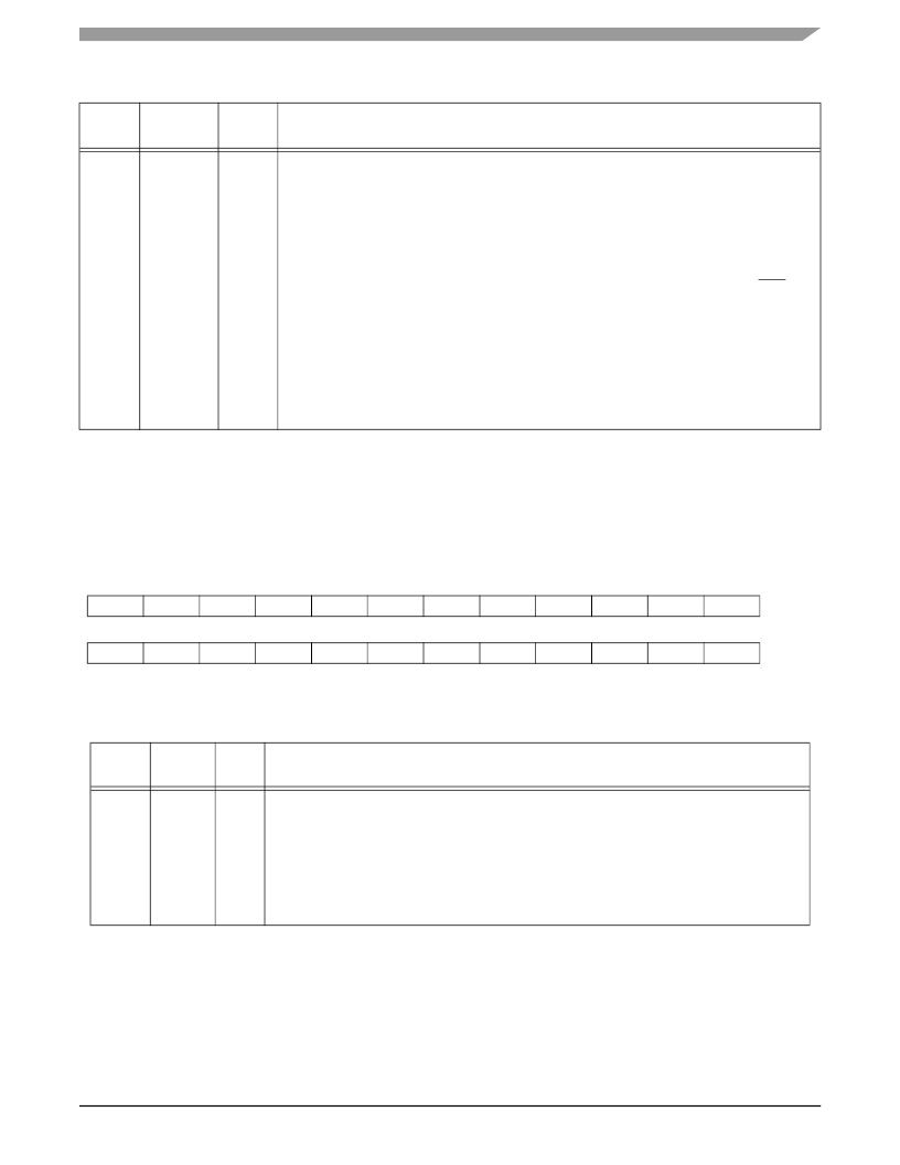
�DMA� Control� Registers� 5–0� (DCR[5–0])�
�Table� 4-10.� Address� Attribute� Registers� (AAR[0–3])� Bit� Definitions�
�Bit�
�Number�
�1–0�
�Bit� Name�
�BAT[1–0]�
�Reset�
�Value�
�0�
�Bus� Access� Type�
�Description�
�Read/write� bits� that� define� the� type� of� external� memory� (DRAM� or� SRAM)� to� access� for� the�
�area� defined� by� the� BAC[11–0],BYEN,� BXEN,� and� BPEN� bits.� The� encoding� of� BAT[1–0]� is:�
�00� =� Reserved�
�01� =� SRAM� access�
�10� =� DRAM� access�
�11� =� Reserved�
�When� the� external� access� type� is� defined� as� a� DRAM� access� (BAT[1–0]� =� 10),� AA/RAS� acts�
�as� a� Row� Address� Strobe� (RAS)� signal.� Otherwise,� it� acts� as� an� Address� Attribute� signal.�
�External� accesses� to� the� default� area� always� execute� as� if� BAT[1–0]� =� 01� (that� is,� SRAM�
�access).� If� Port� A� is� used� for� external� accesses,� the� BAT� bits� in� the� AAR3–0� registers� must�
�be� initialized� to� the� SRAM� access� type� (that� is,� BAT� =� 01)� or� to� the� DRAM� access� type� (that�
�is� BAT� =� 10).� To� ensure� proper� operation� of� Port� A,� this� initialization� must� occur� even� for� an�
�AAR� register� that� is� not� used� during� any� Port� A� access.�
�Note:�
�At� reset,� the� BAT� bits� are� initialized� to� 00.�
�4.7� DMA� Control� Registers� 5–0� (DCR[5–0])�
�The� DMA� Control� Registers� (DCR[5–0])� are� read/write� registers� that� control� the� DMA� operation�
�for� each� of� their� respective� channels.� All� DCR� bits� are� cleared� during� processor� reset.�
�23�
�DE�
�11�
�DRS0�
�22�
�DIE�
�10�
�D3D�
�21�
�DTM2�
�9�
�DAM5�
�20�
�DTM1�
�8�
�DAM4�
�19�
�DTM0�
�7�
�DAM3�
�18�
�DPR1�
�6�
�DAM2�
�17�
�DPR0�
�5�
�DAM1�
�16�
�DCON�
�4�
�DAM0�
�15�
�DRS4�
�3�
�DDS1�
�14�
�DRS3�
�2�
�DDS0�
�13�
�DRS2�
�1�
�DSS1�
�12�
�DRS1�
�0�
�DSS0�
�Figure� 4-9.� DMA� Control� Register� (DCR)�
�Table� 4-11.� DMA� Control� Register� (DCR)� Bit� Definitions�
�Bit�
�Number�
�23�
�Bit� Name�
�DE�
�Reset�
�Value�
�0�
�DMA� Channel� Enable�
�Description�
�Enables� the� channel� operation.� Setting� DE� either� triggers� a� single� block� DMA� transfer� in� the�
�DMA� transfer� mode� that� uses� DE� as� a� trigger� or� enables� a� single-block,� single-line,� or�
�single-word� DMA� transfer� in� the� transfer� modes� that� use� a� requesting� device� as� a� trigger.� DE�
�is� cleared� by� the� end� of� DMA� transfer� in� some� of� the� transfer� modes� defined� by� the� DTM� bits.�
�If� software� explicitly� clears� DE� during� a� DMA� operation,� the� channel� operation� stops� only�
�after� the� current� DMA� transfer� completes� (that� is,� the� current� word� is� stored� into� the�
�destination).�
�DSP56311� User’s� Manual,� Rev.� 2�
�Freescale� Semiconductor�
�4-27�
�发布紧急采购,3分钟左右您将得到回复。
相关PDF资料
DSPAUDIOEVMMB1E
BOARD MOTHER DSP563XX
DSPIC30F2010 DEVELOPMENT KIT
KIT DEV EMBEDDED C
DSTRM-KT-0181A
DSTREAM DEBUG AND TRACE UNIT
DSUT1CSU
SURGE SUPPR NETWORK W/GROUND
DTEL2
SURGE SUPPRESSOR PHONE RJ11/RJ45
DV003001
PROGRAMMER PICSTART PLUS 16C/17C
DV164035
MPLAB ICD3 IN-CIRC DEBUGGER
DV164039
KIT DEV PIC24FJ256DA210
相关代理商/技术参数
DSP56311EVMIG_D
制造商:未知厂家 制造商全称:未知厂家 功能描述:DSP56311EVMIG DSP56311EVM Sample Code
DSP56311EVMUM
制造商:未知厂家 制造商全称:未知厂家 功能描述:DSP56311 Evaluation Module Hardware Reference Manual
DSP56311FACT
制造商:未知厂家 制造商全称:未知厂家 功能描述:DSP56311 Higher performance programmable DSP for demanding voice and data applications
DSP56311UM
制造商:未知厂家 制造商全称:未知厂家 功能描述:DSP56311 24-Bit Digital Signal Processor Users Manual
DSP56311UMAD
制造商:未知厂家 制造商全称:未知厂家 功能描述:DSP56311 Users Manual Addendum
DSP56311VF150
功能描述:数字信号处理器和控制器 - DSP, DSC 150Mhz/300MMACS 150Mhz EFCOP RoHS:否 制造商:Microchip Technology 核心:dsPIC 数据总线宽度:16 bit 程序存储器大小:16 KB 数据 RAM 大小:2 KB 最大时钟频率:40 MHz 可编程输入/输出端数量:35 定时器数量:3 设备每秒兆指令数:50 MIPs 工作电源电压:3.3 V 最大工作温度:+ 85 C 封装 / 箱体:TQFP-44 安装风格:SMD/SMT
DSP56311VF150B1
功能描述:数字信号处理器和控制器 - DSP, DSC 24 BIT DSP
RoHS:否 制造商:Microchip Technology 核心:dsPIC 数据总线宽度:16 bit 程序存储器大小:16 KB 数据 RAM 大小:2 KB 最大时钟频率:40 MHz 可编程输入/输出端数量:35 定时器数量:3 设备每秒兆指令数:50 MIPs 工作电源电压:3.3 V 最大工作温度:+ 85 C 封装 / 箱体:TQFP-44 安装风格:SMD/SMT
DSP56311VF150R2
功能描述:数字信号处理器和控制器 - DSP, DSC 24 BIT DSP RoHS:否 制造商:Microchip Technology 核心:dsPIC 数据总线宽度:16 bit 程序存储器大小:16 KB 数据 RAM 大小:2 KB 最大时钟频率:40 MHz 可编程输入/输出端数量:35 定时器数量:3 设备每秒兆指令数:50 MIPs 工作电源电压:3.3 V 最大工作温度:+ 85 C 封装 / 箱体:TQFP-44 安装风格:SMD/SMT